Google TPU 8tx and 8i Max Release: Confidential, Big Context
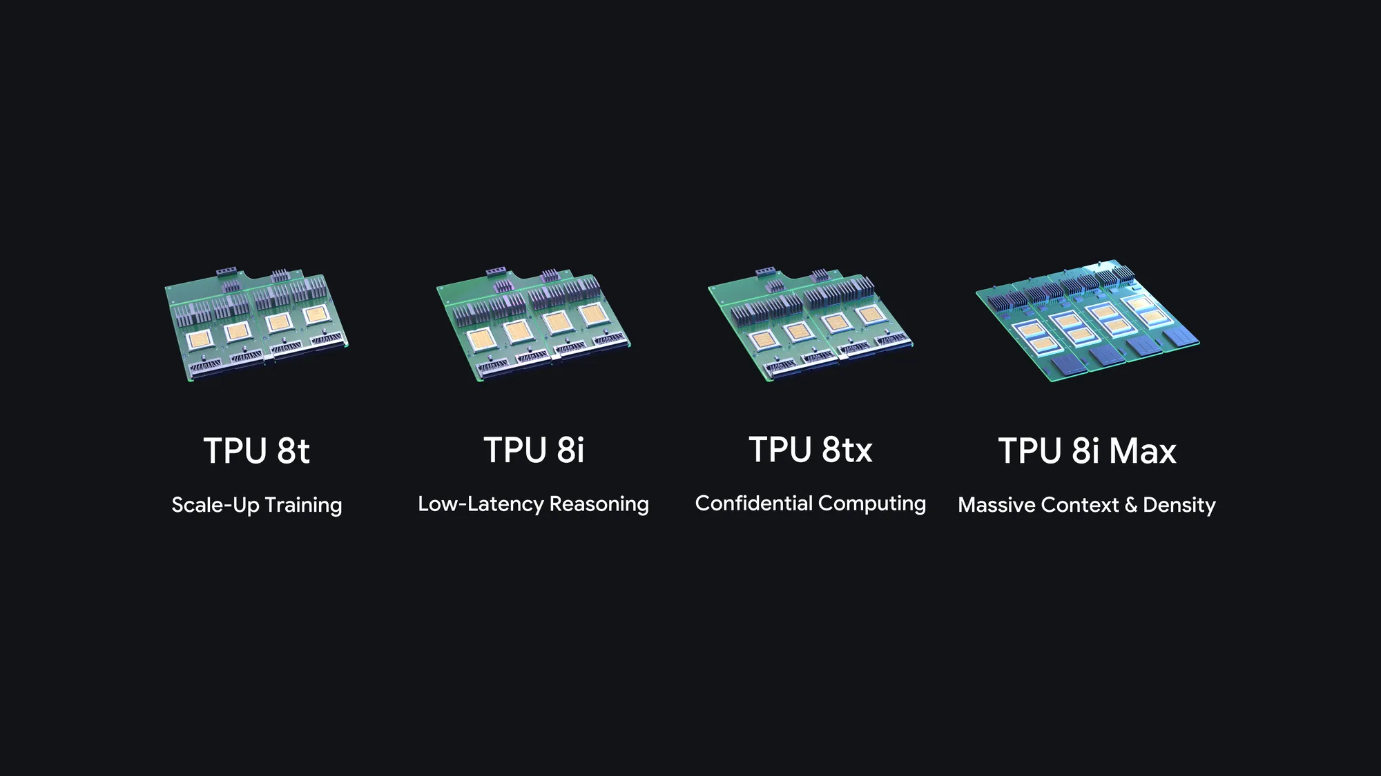
Google used its official blog on November 9, 2026 to add two systems to the eighth TPU generation. TPU 8tx is a third system built for security and confidential inference. TPU 8i Max is a fourth system that packages two TPU 8i chips in one package. Google said this is the first time it has released four TPU systems in one year, and it put the TPU customer count at close to 100 organisations, spanning frontier labs, trading firms, retailers and universities.
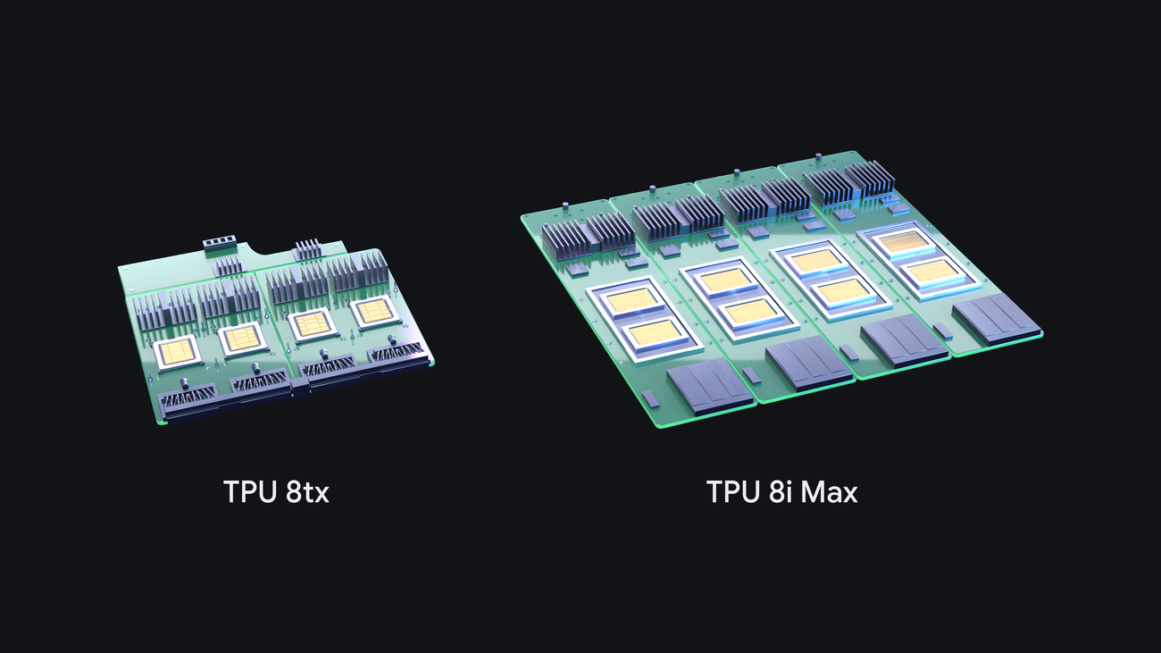
Neither system is a new chip design, and that is the interesting part. TPU 8tx reuses the silicon of TPU 8t and changes the host, the network and the security posture around it. TPU 8i Max reuses TPU 8i silicon and changes the packaging. Google describes this approach as building the computer around the chip. In practice it means the generation now splits by workload constraint rather than by raw compute alone: training, low latency inference, confidential computing and massive context each get a dedicated system.
TPU 8tx and Confidential Inference
TPU 8tx pairs the same silicon as TPU 8t with a fifth generation AMD EPYC host CPU. Google says the system protects data in use and model weights at the hardware layer. That protection targets the gap that ordinary encryption leaves open: data is encrypted at rest and in transit in most cloud setups, but it sits exposed in memory while a model actually processes it. For a hospital, a bank or a lab running proprietary models on sensitive data, that in-use window is often the part a compliance review asks about first.
The network changes with the security posture. TPU 8tx adopts a Boardfly network that Google says delivers up to 2x lower latency than TPU 8t with almost no performance loss. The workloads Google names for the system are fine-tuning, large model distillation and reinforcement learning agent training on sensitive data, all on one system instead of moving the data to a separate cluster. Keeping the data in place matters as much as the protection itself, because every copy to another cluster is another surface a security team has to approve.
TPU 8i Max and the Two-Chip Package
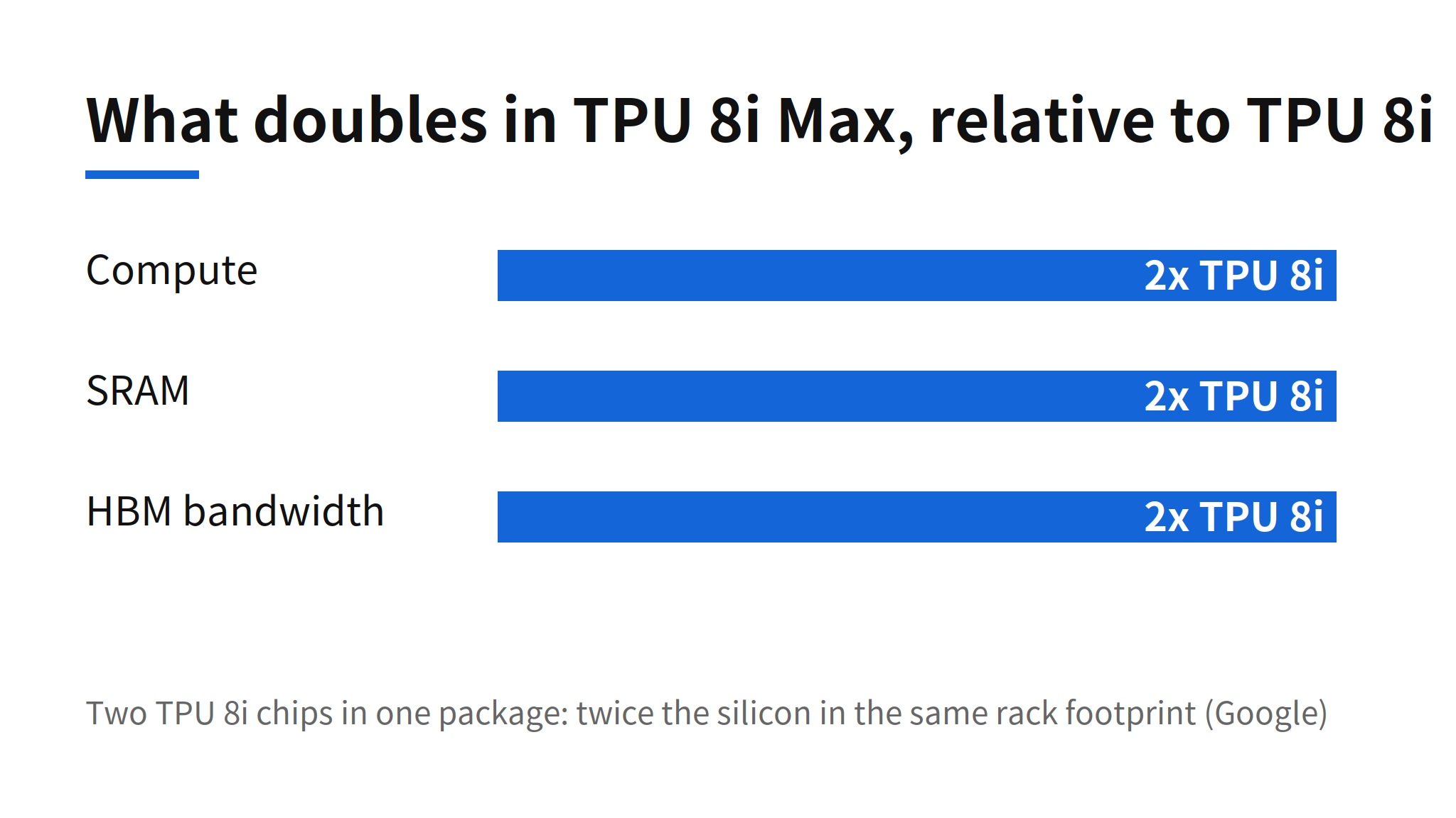
TPU 8i Max takes the direct route to more capacity: two TPU 8i chips in a single package. Compute, SRAM and HBM bandwidth all come out at 2x TPU 8i, and Google frames the gain as twice the silicon inside the same rack footprint. Rack footprint is the binding constraint in most data centres, so density per rack is a more useful number for capacity planning than performance per chip.
Google positions the system for massive context, and the reasoning tracks where agent workloads are heading. Agents that move across an entire codebase carry large working sets, and the context has to stay close to the compute or latency eats the gain. A package that doubles SRAM and HBM bandwidth along with compute keeps that balance instead of widening one side only. Whether real workloads scale linearly across the two chips is a separate question, and the announcement offers no independent benchmark to answer it.
Lineup Expansion From Two Systems to Four
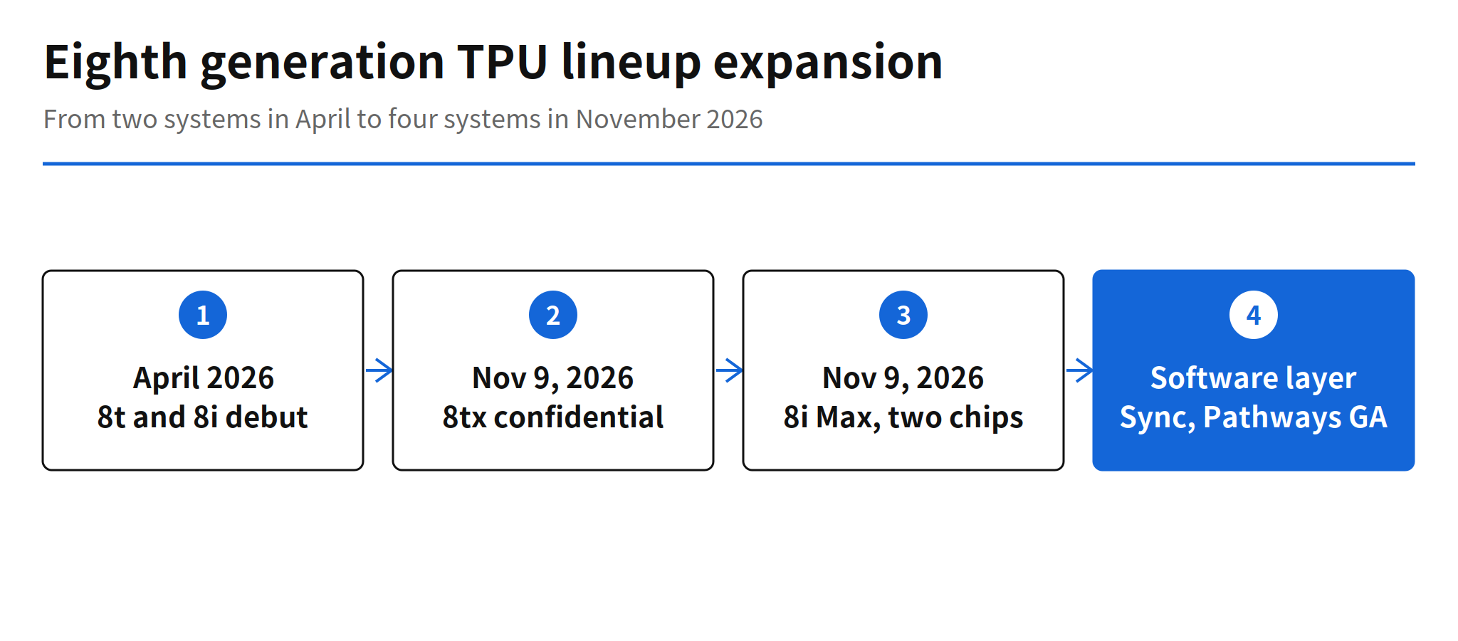
The eighth generation opened in April 2026 at Google Cloud Next with two systems: TPU 8t for training and TPU 8i for realtime inference. Google quoted up to 2.7x training performance over the previous generation and an 80% improvement in inference price performance at that launch. The November additions do not revise those silicon numbers. They widen the range sideways, into confidential computing and context density, which is a different kind of expansion from a faster chip.
TPU Sync, Pathways and Dynamic Slicing
The same post moved several software pieces forward. Google said it will open source TPU Sync, a model state layer that ties chip HBM, host DRAM and shared storage into a single memory tier. Google says it cuts KV transfer latency and time to first token by more than 90%. A unified memory tier attacks the same bottleneck as the 8i Max packaging, from the software side: state that has to move between tiers on every step is state that decides how large a context is practical.
Cloud Pathways reached general availability on GKE, and GKE dynamic slicing reached general availability as well. Google says dynamic slicing makes job start times up to 5x faster and failure recovery up to 4.5x faster. An open source TPU agent suite also arrived in preview, connecting to Claude Code, Cursor and Google Antigravity to automate TPU onboarding and kernel auto-tuning. The pattern across all three is operational: as the hardware range fragments into four specialised systems, the software layer has to absorb more of the scheduling, memory and tuning work, or the specialisation becomes a burden on the teams using it.
Open Questions and Limits
- No price or availability date. The official post gives neither for TPU 8tx or TPU 8i Max. Secondary coverage citing Bloomberg reporting pointed to availability in 2027, but Google has not confirmed that timing.
- Vendor figures only. The up to 2x latency cut for Boardfly and the more than 90% cut in KV transfer latency and time to first token are Google figures. The announcement includes no independent benchmark of the new systems.
- Security detail is thin. The post does not explain how the confidential computing on TPU 8tx is verified, which is the detail a regulated buyer will need before committing sensitive workloads.
Related Reading
For the software side of running PyTorch on these chips, see the earlier report on TorchTPU, the native PyTorch backend for TPUs.
FAQ
What are TPU 8tx and TPU 8i Max?
They are the third and fourth systems in Google's eighth TPU generation, announced on November 9, 2026. TPU 8tx is built for security and confidential inference on the same silicon as TPU 8t. TPU 8i Max packages two TPU 8i chips in one package for large context workloads. Google said this is the first time it has released four TPU systems in a single year.
How does TPU 8tx protect sensitive workloads?
TPU 8tx pairs TPU 8t silicon with a fifth generation AMD EPYC host CPU and protects data in use and model weights at the hardware layer, according to Google. Its Boardfly network cuts latency by up to 2x compared with TPU 8t with almost no performance loss. Google did not disclose how the confidential computing is verified.
How much bigger is TPU 8i Max than TPU 8i?
Compute, SRAM and HBM bandwidth are all twice those of TPU 8i, because the package holds two TPU 8i chips. Google describes the result as twice the silicon inside the same rack footprint, aimed at massive context workloads.
When will TPU 8tx and TPU 8i Max be available, and at what price?
The official Google post gives no price and no availability date for either system. Secondary coverage citing Bloomberg reporting pointed to availability in 2027, but Google has not confirmed that timing, so it should be treated as unconfirmed.